SERVICE MANUAL
HC
NSX-AK772
COMPACT DISC STEREO
CASSETTE RECEIVER
BASIC TAPE MECHANISM: 2ZM-3MK2YPR4N
BASIC CD MECHANISM: 4ZG-1 VOS1DSH
If requiring information about the CD mechanism, see Service Manual of 4ZG-1,
S/M Code No.09-985-249-8OT.
S/M Code No. 09-989-293-9OT
REVISION
SYSTEM
NSX-AK772
CD-CASSEIVER
CX-NAK772
SPEAKER
SX-NAV704
SX-CR675
aiwa

TABLE OF CONTENTS
SPECIFICATIONS ................................................................................................................ 3
NOTICE BEFORE STARTING REPAIR ................................................................................. 4,5
PROTECTION OF EYES FROM LASER BEAM DURING SERVICING............................................ 6
PRECAUTION TO REPLACE OPTICAL BLOCK ........................................................................ 6
ELECTRICAL MAIN PARTS LIST ................................................................................... 7 ~ 12
TRANSISTOR ILLUSTRATION .............................................................................................. 13
BLOCK DIAGRAM 1 (PRO) .............................................................................................. 14
BLOCK DIAGRAM 2 (MAIN / FRONT) ........................................................................... 15, 16
WIRING 1 (MAIN) ...................................................................................................... 17, 18
SCHEMATIC DIAGRAM 1 (MAIN 1/2) .......................................................................... 19, 20
WIRING 2-1 (FRONT) .................................................................................................. 21, 22
WIRING 2-2 (FRONT) .................................................................................................. 23, 24
SCHEMATIC DIAGRAM 2 (FRONT) .............................................................................. 25, 26
SCHEMATIC DIAGRAM 3 (MAIN 2/2) .......................................................................... 27, 28
WIRING 3 (PRO) ........................................................................................................ 29, 30
SCHEMATIC DIAGRAM 4 (PRO) .................................................................................. 31, 32
WIRING 4 (SW) .............................................................................................................. 33
WIRING 5 (AC1 / AC2) .................................................................................................... 34
WIRING 6 (DECK) ........................................................................................................... 35
SCHEMATIC DIAGRAM 5 (TUNER FRONT END) .................................................................. 36
IC BLOCK DIAGRAM .................................................................................................. 37 ~ 43
IC DESCRIPTION .......................................................................................................... 44, 45
FL GRID ASSIGNMENT & ANODE CONNECTION................................................................. 46, 47
ADJUSTMENT <TUNER / DECK> .................................................................................... 48, 49
PRACTICAL SERVICE FIGURE ............................................................................................. 50
MECHANICAL EXPLODED VIEW 1 / 1 ............................................................................ 51, 52
MECHANICAL PARTS LIST 1 / 1 ........................................................................................ 53
TAPE MECHANISM EXPLODED VIEW 1 / 1 .................................................................... 54, 55
TAPE MECHANISM PARTS LIST 1 / 1 ................................................................................ 56
SPRING APPLICATION POSITION ....................................................................................... 57
SPEAKER DISASSEMBLY INSTRUCTIONS ............................................................................... 58
SPEAKER PARTS LIST ......................................................................................................... 59
ACCESSORIES / PACKAGE LIST .......................................................................................... 59
REFERENCE NAME LIST ..................................................................................................... 60
2

<FM Tuner section>
Tuning range
87.5 MHz to 108 MHz
Usable sensitivity(IHF)
13.2dBf
Antenna terminals
75 ohms (unbalanced)
<MW Tuner section>
Tuning range
531 kHz to 1602 kHz
(9 kHz step)
530 kHz to 1710 kHz
(10 kHz step)
Usable sensitivity
350uV/m
Antenna
Loop antenna
<SW Tuner section>
Tuning range
5.900 MHz to 17.900 MHz
Antenna
Wire antenna
<Amplifier section>
Power output
Front
Rated : 80 W + 80 W
(6 ohms, THD 1%, 1 kHz)
Reference : 100 W + 100 W
(6 ohms, THD 10%, 1 kHz)
Rear (Surround)
Rated : 33 W + 33 W
(8 ohms, THD 1%, 1 kHz)
Reference : 40 W + 40 W
(8 ohms, THD 10%, 1 kHz)
Center
Rated : 33 W
(8 ohms, THD 1%, 1 kHz)
Reference : 40 W
(8 ohms, THD 10%, 1 kHz)
Total harmonic distortion
0.05% (50 W, 1 kHz,
6 ohms, DIN AUDIO / Front)
Inputs
VIDEO/AUX : 210 mV
(adjustable)
MD : 210mV (adjustable)
MIC1, MIC2 : 1.4mV
(10 kohms)
5.1 CH INPUT
FRONT (L,R) : 560 mV
REAR (L,R) : 320 mV
CENTER : 300 mV
SUB WOOFER : 400 mV
Outputs
LINE OUT: 280mV
VIDEO OUT: 1.0 Vp-p
(75 ohms)
SUB WOOFER : 1 V
SPEAKERS: accept
speakers of 6 ohms or more
SURROUND SPEAKERS:
accept speakers of 8 ohms to
16 ohms
CENTER SPEAKER:
accept speakers of 8 ohms
or more
PHONES (stereo jack) :
accepts headphones of 32
ohms or more
<Cassette deck section>
Track format
4 tracks, 2 channels stereo
Frequency response
CrO2 tape : 50 Hz 16000 Hz
Normaltape : 50 Hz 15000
Hz
Recording system
AC bias
Heads
Deck 1 : Playback head x 1
Deck 2 : Recording/playback
head x 1/ erase
head x 1
SPECIFICATIONS
<Compact disc player section>
Laser
Semiconductor laser
(=780nm)
D-A converter
1 bit dual
Signal-to-noise ratio
85 dB (1 kHz, 0 dB)
Harmonic distortion
0.05 % (1 kHz, 0 dB)
Wow and flutter
Unmeasurable
Video signal
NTSC/PAL color format
(selectable)
Video data
MPEG 1
Audio data
MPEG 1, LAYER 2
<Speakersystem>SXNAV704
Cabinet type
2 way, bass reflex (magnetic
shielded type)
Speakers
Woofer : 160 mm cone type
Tweeter : 80 mm cone type
Impedance
6 ohms
Output sound pressure level87dB/W/m
Dimensions (W x H x D)
235 x 324 x 260 mm
Weight
5.4 kg
<General>
Power requirements
120 V/220 - 230 V/240 V AC
switchable, 50/60 Hz
Power consumption
210W
Dimensions of main unit
260 x 324 x 348 mm
Weight of main unit
8.9 kg
Design and specifications are subject to change without
notice.
The word "BBE"and the "BBE symbol" are trademarks of
BBE Sound, Inc.
Under license from BBE Sound,Inc.
DOLBY NR / DOLBY PRO LOGIC
Manufactured under license from Dolby Laboratories
Licensing Corporation.
"DOLBY", and the double-D symbol
and "PRO LOGIC"
are trademarks of Dolby Laboratories Licensing
Corporation.
3
NOTE ON BEFORE STARTING REPAIR
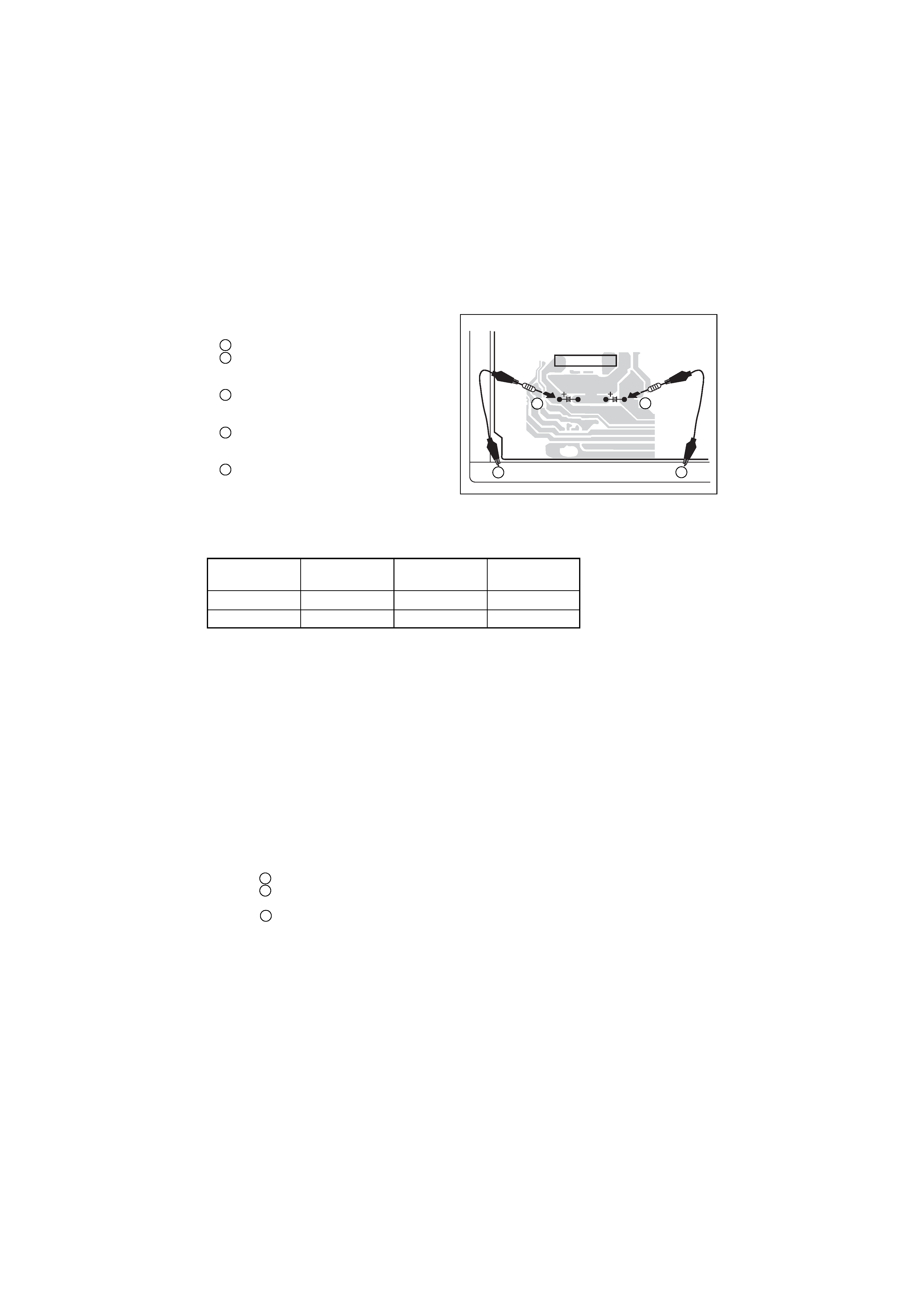
Fig-1
MAIN C.B
D101
C101
C102
22
34
Charging voltage (V)
Discharging
Rated power (W)
Parts number
(C101, 102)
resistor (ohm)
25-48
100
3
87-A00-247-090
49-140
220
5
87-A00-232-090
1. Forced discharge of electrolytic capacitor of power supply block
When repair is going to be attempted in the set that uses relay circuit in the power supply block, electric potential is kept
charged across the electrolytic capacitors (C101, 102) even though AC power cord is removed. If repair is attempted in this
condition, the secondary defect can occur.
In order to prevent the secondary trouble, perform the following measures before starting repair work.
Discharge procedure
1
Remove the AC power cord.
2
Connect a discharging resistor at an end of lead
wire that has clips at both ends. Connector the
other end of the lead wire to metal chassis.
3
Contact the other end of the discharging resistor
to the positive (+) side (+VH) of C101. (For two
seconds)
4
Contact the same end of the discharging resistor
as step 3 to the negative (-) side (-VH) of C102
in the same way. (For two seconds)
5
Check that voltage across C101 and C102 has
decreased 1 V or less using a multimeter or an
oscilloscope.
Select a discharging resistor referring to the following table.
Note: The reference numbers (C101, C102) of the electrolytic capacitors can change depending on the models. Be sure to check
the reference numbers of the charging capacitor on schematic diagram before starting the discharging work.
2. Check items before exchanging the MICROCOMPUTER
Be sure to check the following items before exchanging the MICROCOMPUTER. Exchange the MICROCOMPUTER after
confirming that the MICROCOMPUTER is surely defective.
2-1. Regarding the HOLD terminal of the MICROCOMPUTER
When the HOLD terminal (INPUT) of the MICROCOMPUTER is H, the MICROCOMPUTER is judged to be
operating correctly. When this terminal is L, the main power cannot be turned on. Therefore, be sure to check the
terminal voltage of the HOLD terminal before exchange.
When the MICROCOMPUTER is not defective, the HOLD terminal can also go L when the POWER AMPLIFIER
has any abnormalities that triggers the abnormality detection circuit on the MAIN C. B. that sets the HOLD terminal to
L.
Good or no good judgment of the MICROCOMPUTER
1
Turn on the AC main power.
2
Confirm that the main power is turned on and the HOLD terminal of the MICROCOMPUTER keeps the H
level or not.
3
When the HOLD terminal is L level, the abnormality detection circuit is judged to be working correctly and
the MICROCOMPUTER is judged to be good.
4
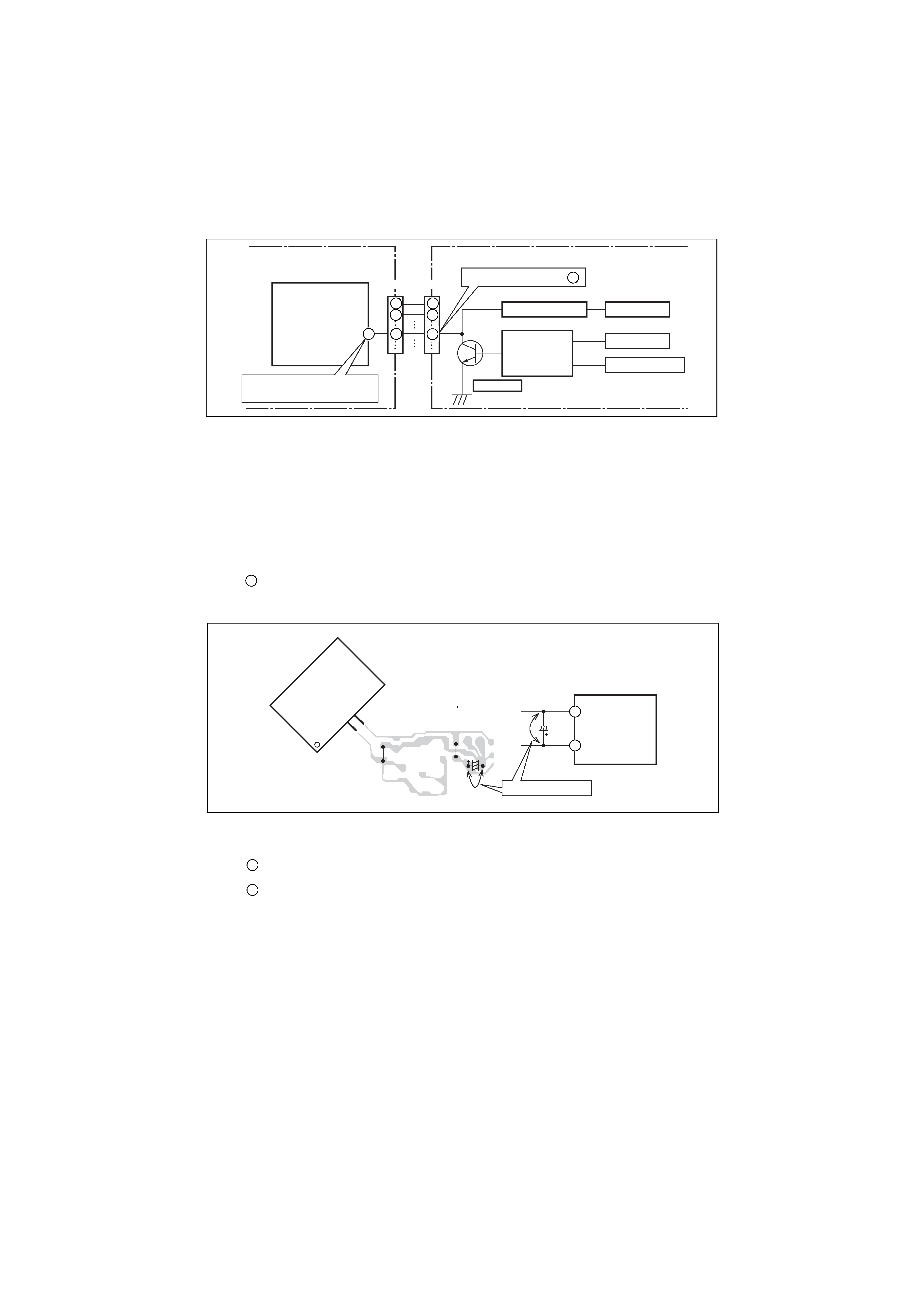
MICRO-
COMPUTER
MICROCOMPUTER
FRONT C.B
FRONT C.B
VSS
VDD
C113
*
%
C113
18
15
Short with tweezers.
Fig-2-2
In such a case, check also if the POWER AMPLIFIER circuit or power supply circuit has any abnormalities or
not.
2-2. Regarding reset
There are cases that the machine does not work correctly because the MICROCOMPUTER is not reset even though the
AC power cord is re-inserted, or the software reset (pressing the STOP key + POWER key) is performed.
When the above described phenomenon occurs, it can leads to wrong judgment as if the MICROCOMPUTER is
defective and to exchange the MICROCOMPUTER. In such a case, perform the forced-reset by the following
procedure and check good or no good of the MICROCOMPUTER.
1
Remove the AC power cord.
2
Short the both ends of the electrolytic capacitor C113 that is connected to VDD of the MICROCOMPUTER with
tweezers.
3
Connect the AC power cord again. If the MICROCOMPUTER returns to the normal operation, the
MICROCOMPUTER is good.
Note: The reference number or MICROCOMPUTER pin number of transistor (Q110) and electrolytic capacitor (C113) can
change depending on the models. Be sure to check the reference numbers on schematic diagram before starting the
discharging work.
2-3.Confirmation of soldering state of MICROCOMPUTER
Check the soldering state of the MICROCOMPUTER in addition to the above described procedures. Be sure to
exchange the MICROCOMPUTER after surely confirming that the trouble is not caused by poor soldering but the
MICROCOMPUTER itself.
Fig-2-1
MICROCOMPUTER
FRONT C.B
MAIN C.B
OVER LOAD DET
DC DET
Q110
POWER AMP
POWER AMP
POWER SUPPLY
HOLD
HOLD SW
(
AC DET
PIN101 CON601
1
2
*
1
2
*
In some models, it is PIN (.
PIN number is different
depending upon microprocessor.
5
15
18
19
18
18
1
2
1
2
19 .
PIN101
CON601